Click for more.
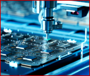
The US Department of Commerce today published a Notice of Intent (NOI) to open a competition for new research and development (R&D) activities that it said will establish and accelerate domestic capacity for semiconductor advanced packaging. The CHIPS for America program predicts that up to $1.6 billion in funding will go to five R&D areas.* These were first outlined in the vision for the National Advanced Packaging Manufacturing Program (NAPMP).** Through potential cooperative agreements, CHIPS for America would make several awards of ~$150 million federal funding per award in each research area.
“President Biden was clear that we need to build a vibrant domestic semiconductor ecosystem here in the U.S., and advanced packaging is a huge part of that. Now, thanks to the Biden-Harris Administration’s commitment to investing in America, the U.S. will have multiple advanced packaging options across the country and push the envelope in new packaging technologies. This announcement is just the most recent example of our commitment to investing in cutting edge R&D that is critical to creating quality jobs in the U.S. and making our country a leader in advanced semiconductor manufacturing.” said U.S. Secretary of Commerce Gina Raimondo.
Funding actions are projected to be relevant to one or more five R&D areas:
- Equipment, tools, processes, and process integration;
- Power delivery and thermal management;
- Connector technology, including photonics and radio frequency (RF);
- Chiplets ecosystem;
- and co-design/electronic design automation (EDA).
“The National Advanced Packaging Manufacturing Program will enable a packaging sector within the United States that outpaces the world through innovation driven by robust R&D,” said Under Secretary of Commerce for Standards and Technology and National Institute of Standards and Technology (NIST) Director Laurie E. Locascio. “Within a decade, through R&D funded by CHIPS for America, we will create a domestic packaging industry where advanced node chips manufactured in the U.S. and abroad can be packaged within the United States and where innovative designs and architectures are enabled through leading-edge packaging capabilities.
“Under President Biden’s leadership, we’re bringing semiconductor manufacturing back to the United States, teaming with industry to build factories, supply chains, and jobs in communities across the country. That’s how we win today, and CHIPS R&D is how we win tomorrow,” said Arati Prabhakar, Assistant to the President for Science and Technology and Director of the White House Office of Science and Technology Policy. “Investing in research to accelerate new advanced semiconductor packaging approaches will help this pivotal and fast-changing industry thrive here at home now and into the future.”
*About CHIPS for America
CHIPS for America is part of The Biden Administration economic plan to invest in America, stimulate private sector investment, create good-paying jobs, make more in the United States, and revitalize communities left behind. CHIPS for America includes:
- the CHIPS Program Office, responsible for manufacturing incentives.
- the CHIPS Research and Development (R&D) Office, responsible for R&D programs.
Both offices are within the National Institute of Standards and Technology (NIST) at the Department of Commerce. NIST says it “promotes U.S. innovation and industrial competitiveness by advancing measurement science, standards, and technology in ways that enhance economic security and improve our quality of life. NIST is uniquely positioned to successfully administer the CHIPS for America program because of the bureau’s strong relationships with U.S. industries, its deep understanding of the semiconductor ecosystem, and its reputation as fair and trusted.”
CHIPS R&D released the first funding opportunity for the National Advanced Packaging Manufacturing Program (NAPMP) in February 2024. That funding opportunity requested applications for R&D activities that will establish and accelerate domestic capacity for advanced packaging substrates and substrate materials, a key technology for manufacturing semiconductors.
Applicants submitted more than100 concept papers, representing 28 states On 22 May 2024, the Department of Commerce announced that eight teams were selected to submit full applications for NAPMP funding for materials and substrate materials. Final projects ae hoped to be central in helping to ensure that American innovation drives cutting-edge developments in semiconductor R&D and manufacturing. The CHIPS for America program anticipates awarding approximately $300 million in amounts up to approximately $100 million over up to 5 years per award. Program awards may be leveraged by voluntary co-investment. Full applications for the first NAPMP funding opportunity were due on 3 July 2024.
**AutoInformed on

About Ken Zino
Ken Zino, editor and publisher of AutoInformed, is a versatile auto industry participant with global experience spanning decades in print and broadcast journalism, as well as social media. He has automobile testing, marketing, public relations and communications experience. He is past president of The International Motor Press Assn, the Detroit Press Club, founding member and first President of the Automotive Press Assn. He is a member of APA, IMPA and the Midwest Automotive Press Assn.
He also brings an historical perspective while citing their contemporary relevance of the work of legendary auto writers such as Ken Purdy, Jim Dunne or Jerry Flint, or writers such as Red Smith, Mark Twain, Thomas Jefferson – all to bring perspective to a chaotic automotive universe.
Above all, decades after he first drove a car, Zino still revels in the sound of the exhaust as the throttle is blipped during a downshift and the driver’s rush that occurs when the entry, apex and exit points of a turn are smoothly and swiftly crossed. It’s the beginning of a perfect lap.
AutoInformed has an editorial philosophy that loves transportation machines of all kinds while promoting critical thinking about the future use of cars and trucks.
Zino builds AutoInformed from his background in automotive journalism starting at Hearst Publishing in New York City on Motor and MotorTech Magazines and car testing where he reviewed hundreds of vehicles in his decade-long stint as the Detroit Bureau Chief of Road & Track magazine. Zino has also worked in Europe, and Asia – now the largest automotive market in the world with China at its center.


Biden Administration – $1.6B in Semiconductor Manufacturing
Click for more.
The US Department of Commerce today published a Notice of Intent (NOI) to open a competition for new research and development (R&D) activities that it said will establish and accelerate domestic capacity for semiconductor advanced packaging. The CHIPS for America program predicts that up to $1.6 billion in funding will go to five R&D areas.* These were first outlined in the vision for the National Advanced Packaging Manufacturing Program (NAPMP).** Through potential cooperative agreements, CHIPS for America would make several awards of ~$150 million federal funding per award in each research area.
“President Biden was clear that we need to build a vibrant domestic semiconductor ecosystem here in the U.S., and advanced packaging is a huge part of that. Now, thanks to the Biden-Harris Administration’s commitment to investing in America, the U.S. will have multiple advanced packaging options across the country and push the envelope in new packaging technologies. This announcement is just the most recent example of our commitment to investing in cutting edge R&D that is critical to creating quality jobs in the U.S. and making our country a leader in advanced semiconductor manufacturing.” said U.S. Secretary of Commerce Gina Raimondo.
Funding actions are projected to be relevant to one or more five R&D areas:
“The National Advanced Packaging Manufacturing Program will enable a packaging sector within the United States that outpaces the world through innovation driven by robust R&D,” said Under Secretary of Commerce for Standards and Technology and National Institute of Standards and Technology (NIST) Director Laurie E. Locascio. “Within a decade, through R&D funded by CHIPS for America, we will create a domestic packaging industry where advanced node chips manufactured in the U.S. and abroad can be packaged within the United States and where innovative designs and architectures are enabled through leading-edge packaging capabilities.
“Under President Biden’s leadership, we’re bringing semiconductor manufacturing back to the United States, teaming with industry to build factories, supply chains, and jobs in communities across the country. That’s how we win today, and CHIPS R&D is how we win tomorrow,” said Arati Prabhakar, Assistant to the President for Science and Technology and Director of the White House Office of Science and Technology Policy. “Investing in research to accelerate new advanced semiconductor packaging approaches will help this pivotal and fast-changing industry thrive here at home now and into the future.”
*About CHIPS for America
CHIPS for America is part of The Biden Administration economic plan to invest in America, stimulate private sector investment, create good-paying jobs, make more in the United States, and revitalize communities left behind. CHIPS for America includes:
Both offices are within the National Institute of Standards and Technology (NIST) at the Department of Commerce. NIST says it “promotes U.S. innovation and industrial competitiveness by advancing measurement science, standards, and technology in ways that enhance economic security and improve our quality of life. NIST is uniquely positioned to successfully administer the CHIPS for America program because of the bureau’s strong relationships with U.S. industries, its deep understanding of the semiconductor ecosystem, and its reputation as fair and trusted.”
CHIPS R&D released the first funding opportunity for the National Advanced Packaging Manufacturing Program (NAPMP) in February 2024. That funding opportunity requested applications for R&D activities that will establish and accelerate domestic capacity for advanced packaging substrates and substrate materials, a key technology for manufacturing semiconductors.
Applicants submitted more than100 concept papers, representing 28 states On 22 May 2024, the Department of Commerce announced that eight teams were selected to submit full applications for NAPMP funding for materials and substrate materials. Final projects ae hoped to be central in helping to ensure that American innovation drives cutting-edge developments in semiconductor R&D and manufacturing. The CHIPS for America program anticipates awarding approximately $300 million in amounts up to approximately $100 million over up to 5 years per award. Program awards may be leveraged by voluntary co-investment. Full applications for the first NAPMP funding opportunity were due on 3 July 2024.
**AutoInformed on
About Ken Zino
Ken Zino, editor and publisher of AutoInformed, is a versatile auto industry participant with global experience spanning decades in print and broadcast journalism, as well as social media. He has automobile testing, marketing, public relations and communications experience. He is past president of The International Motor Press Assn, the Detroit Press Club, founding member and first President of the Automotive Press Assn. He is a member of APA, IMPA and the Midwest Automotive Press Assn. He also brings an historical perspective while citing their contemporary relevance of the work of legendary auto writers such as Ken Purdy, Jim Dunne or Jerry Flint, or writers such as Red Smith, Mark Twain, Thomas Jefferson – all to bring perspective to a chaotic automotive universe. Above all, decades after he first drove a car, Zino still revels in the sound of the exhaust as the throttle is blipped during a downshift and the driver’s rush that occurs when the entry, apex and exit points of a turn are smoothly and swiftly crossed. It’s the beginning of a perfect lap. AutoInformed has an editorial philosophy that loves transportation machines of all kinds while promoting critical thinking about the future use of cars and trucks. Zino builds AutoInformed from his background in automotive journalism starting at Hearst Publishing in New York City on Motor and MotorTech Magazines and car testing where he reviewed hundreds of vehicles in his decade-long stint as the Detroit Bureau Chief of Road & Track magazine. Zino has also worked in Europe, and Asia – now the largest automotive market in the world with China at its center.